Aluminum Substrate Cut
Aluminum Substrate Cut – Precision Laser Processing
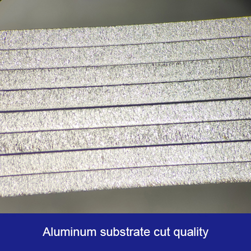
This is a high-precision laser system for cutting aluminum substrates, ideal for electronics and medical applications, ensuring superior cut quality.
The Aluminum Substrate Cut system from AQ-Laser is an advanced laser processing solution designed for high-precision cutting of aluminum substrates used in electronics manufacturing. Tailored for industries such as medical device production, telecommunications, and consumer electronics, this system delivers clean, burr-free cuts with minimal thermal impact, ensuring exceptional edge quality. It is optimized for processing aluminum substrates, enabling intricate circuit designs and high-density interconnects (HDI) critical for high-performance applications. Equipped with automated features like precise positioning and focusing, it ensures efficient, high-quality production for advanced electronic components.
תכונות עיקריות:
- High-Precision Cutting: Achieves cutting accuracy of ≤±10μm and seam widths of 15–30μm for intricate, burr-free designs.
- Material Optimization: Processes aluminum substrates with excellent thermal conductivity and lightweight properties.
- Low Thermal Impact: Advanced fiber laser technology minimizes heat-affected zones, preserving material integrity.
- Automated Efficiency: Includes automatic positioning, focusing, and feeding systems for streamlined production.
- CleanCut Technology: Ensures carbonization-free edges, enhancing technical cleanliness and reliability.
- עמידות בפני קורוזיה: Supports durable aluminum substrates resistant to environmental degradation.
Certification and Standards:
Certified to ISO9001 and IATF16949 standards, ensuring consistent quality for electronics and automotive applications. Compliant with CE marking and RoHS directives for safety and environmental sustainability.
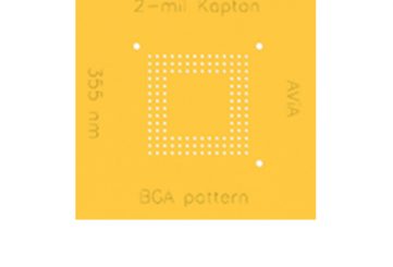
Aluminum Substrate:
- Excellent Thermal Conductivity: Efficiently dissipates heat, ideal for high-power electronics like LED lighting and medical imaging devices.
- Lightweight: Reduces overall device weight, enhancing portability for applications in wearables and compact electronics.
- Cost-Effective: Offers a balance of performance and affordability, suitable for large-scale electronics manufacturing.
- Corrosion Resistance: Resists environmental degradation, ensuring durability in harsh conditions.
- Mechanical Strength: Provides robust support for circuit components, maintaining structural integrity under stress.
- Recyclability: Environmentally friendly, supporting sustainable manufacturing practices.
Copper Substrate:
- Superior Electrical Conductivity: Ensures efficient signal transmission, critical for high-frequency 5G antennas and power electronics.
- High Thermal Conductivity: Effectively manages heat dissipation, ideal for high-performance PCBs and medical devices.
- Ductility: Allows precise forming and shaping, enabling intricate designs for compact electronic assemblies.
- Durability: Resists wear and tear, providing long-term reliability in demanding applications.
- Solderability: Facilitates strong, reliable connections in circuit assembly, enhancing manufacturing efficiency.
- High-Density Interconnect Support: Enables complex, high-density circuit designs for advanced electronics.
Ceramic Substrate:
- Exceptional Thermal Stability: Withstands extreme temperatures, ideal for high-power and high-frequency electronics like RF modules.
- Superior Electrical Insulation: Prevents unwanted conductivity, ensuring reliable performance in sensitive medical and telecom devices.
- High Mechanical Strength: Maintains structural integrity under stress, supporting precision manufacturing of complex designs.
- Chemical Inertness: Resists corrosion from chemicals and environmental factors, ensuring long-term reliability.
- Low Dielectric Loss: Enhances signal integrity, making it perfect for high-frequency applications like 5G and radar systems.
- Biocompatibility: Suitable for medical implants and diagnostic equipment due to its non-reactive properties.
- High-precision cutting of aluminum substrates for medical devices and consumer electronics.
- Contour cutting and marking for high-performance printed circuit boards (PCBs).
- Processing of aluminum substrates for LED lighting and telecommunications equipment.
- Suitable for high-density interconnect (HDI) designs in automotive and aerospace applications.
- Laser Type: High-performance fiber laser
- Cutting Accuracy: ≤±10μm
- Cutting Seam Width: 15–30μm
- Material Compatibility: Aluminum substrates
- Processing Capabilities: Contour cutting, drilling, and marking
- Automation: Automatic positioning, focusing, and feeding systems
- Supported Formats: Gerber, DXF, DWG, SVG, and other 2D CAD formats