Copper Substrate Cutting and Forming
Copper Substrate Cutting and Forming – Precision Laser Processing for High-Conductivity Electronics
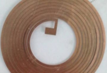
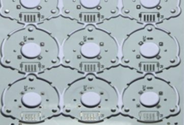
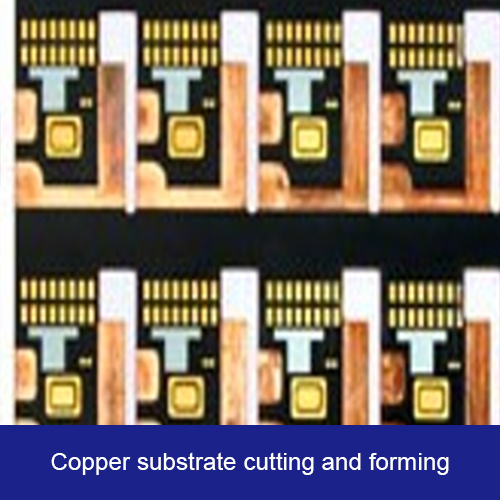
Copper Substrate Cutting and Forming is a high-precision laser machining process designed to create intricate components from copper substrates for medical and electronic applications. Utilizing advanced fiber laser technology with nitrogen assist, this process delivers clean, burr-free cuts and precise forming with minimal thermal distortion. Crafted from high-quality copper, known for its superior electrical and thermal conductivity, the resulting components are ideal for medical sensors, electronic circuits, and high-performance interconnects. The laser-cut design ensures smooth edges and complex patterns, optimizing performance in demanding environments. Tailored for high-precision applications, this process meets the rigorous standards of modern healthcare and electronics manufacturing.
תכונות עיקריות:
- Ultra-Precise Cutting: Seam width of 15–30 µm with machining accuracy of ≤±10 µm for intricate circuit designs.
- Burr-Free Edges: Smooth surfaces ensure reliable performance and safe integration in sensitive applications.
- High Conductivity: Copper substrates provide excellent electrical and thermal conductivity for high-performance electronics.
- Minimal Thermal Impact: Fiber laser with nitrogen assist minimizes oxidation and thermal distortion for enhanced material integrity.
- רבגוניות חומרית: Compatible with copper foils and copper-clad laminates for diverse applications.
- Automated Production: Direct-drive XY motion platform ensures high efficiency and consistent quality.
Certification and Standards:
Certified under ISO 9001 and IATF 16949 for quality management. Compliant with CE and FDA regulations for medical device safety and efficacy.
Aluminum Substrate:
- Excellent Thermal Conductivity: Efficiently dissipates heat, ideal for high-power electronics like LED lighting and medical imaging devices.
- Lightweight: Reduces overall device weight, enhancing portability for applications in wearables and compact electronics.
- Cost-Effective: Offers a balance of performance and affordability, suitable for large-scale electronics manufacturing.
- Corrosion Resistance: Resists environmental degradation, ensuring durability in harsh conditions.
- Mechanical Strength: Provides robust support for circuit components, maintaining structural integrity under stress.
- Recyclability: Environmentally friendly, supporting sustainable manufacturing practices.
Copper Substrate:
- Superior Electrical Conductivity: Ensures efficient signal transmission, critical for high-frequency 5G antennas and power electronics.
- High Thermal Conductivity: Effectively manages heat dissipation, ideal for high-performance PCBs and medical devices.
- Ductility: Allows precise forming and shaping, enabling intricate designs for compact electronic assemblies.
- Durability: Resists wear and tear, providing long-term reliability in demanding applications.
- Solderability: Facilitates strong, reliable connections in circuit assembly, enhancing manufacturing efficiency.
- High-Density Interconnect Support: Enables complex, high-density circuit designs for advanced electronics.
Ceramic Substrate:
- Exceptional Thermal Stability: Withstands extreme temperatures, ideal for high-power and high-frequency electronics like RF modules.
- Superior Electrical Insulation: Prevents unwanted conductivity, ensuring reliable performance in sensitive medical and telecom devices.
- High Mechanical Strength: Maintains structural integrity under stress, supporting precision manufacturing of complex designs.
- Chemical Inertness: Resists corrosion from chemicals and environmental factors, ensuring long-term reliability.
- Low Dielectric Loss: Enhances signal integrity, making it perfect for high-frequency applications like 5G and radar systems.
- Biocompatibility: Suitable for medical implants and diagnostic equipment due to its non-reactive properties.
- Medical Sensors: Produces precision components for wearable and diagnostic medical devices.
- Electronic Circuits: Creates intricate layouts for consumer electronics and high-density interconnects.
- Diagnostic Equipment: Supports high-precision substrates for imaging and laboratory devices.
- Industrial Electronics: Used in robust components for control systems and power electronics.
- Medical Device Manufacturing: Incorporated in the production of advanced electronic substrates.
- Material: Copper Foil, Copper-clad Laminates
- Thickness: 0.05–0.5 mm
- Cutting Seam Width: 15–30 µm
- Machining Accuracy: ≤±10 µm
- Surface Roughness: Ra <0.2 µm
- Manufacturing Process: Fiber laser cutting with nitrogen assist and automated feeding
- Operating Temperature: -20°C to 150°C, suitable for high-performance applications
- Degradation: Non-degradable, designed for long-term stability