Тонкая медная подложка WT0.3mm лазерная формовка
- High Adaptability: Compatible with various PCB materials.
- Ergonomic Design: Visual positioning and dynamic monitoring.
- Настраиваемость: поддерживает персонализированные конфигурации и интеллектуальное производство.
- Certified Quality: Complies with ISO9001 and IATF16949 standards.
Описание продукта
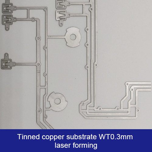
The Тонкая медная подложка WT0.3mm лазерная формовка is a high-precision laser-cut component designed for use in PCB (Printed Circuit Board) applications. Utilizing advanced fiber laser micromachining technology, this copper substrate ensures exceptional accuracy, smooth finishes, and burr-free edges. It is ideal for applications requiring precise and durable PCB substrate solutions.
Основные характеристики:
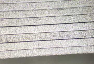
- Высокая точность: Точность резки ≤±10мкм.
- Гладкая отделка: Smooth incision with a seam width of 20~40µm and minimal heat-affected zone.
- Эффективная обработка: Direct-drive mobile double-drive system for one-time cutting.
- Универсальность материала: Compatible with copper substrates and other PCB materials.
- Передовые технологии: Manufactured using 2D and 2.5D CAM software.
Материалы
-
Copper Substrate
-
Aluminum Substrate
-
Ceramic Substrate
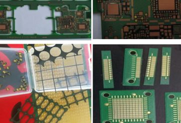
Приложение
The Тонкая медная подложка WT0.3mm лазерная формовка is widely used in the industry for:
-
PCB manufacturing
-
Precision electronics
-
Industrial applications
-
Surface treatment applications