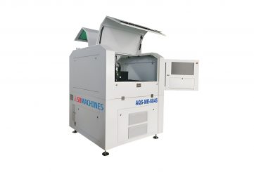
AQS-PCB-6080 Fiber laser cutting machine for precision PCB substrate

AQS-PCB-6080 Fiber Laser Cutting Machine for Precision PCB Substrate – Ultra-fine micromachining for PCB materials
The AQS-PCB-6080 is a fiber laser cutting system developed specifically for high-precision processing of PCB substrates. It handles complex tasks such as cutting, drilling, slotting, and scribing on materials including aluminum, copper, and ceramic substrates. The machine architecture combines stable motion systems, precise laser control, and thermal management to deliver consistent micro-machining quality.
With its compact footprint and robust design, the AQS-PCB-6080 is well suited for cleanroom or electronics production environments. Its control features and modular expandability make it a dependable solution for manufacturers of PCBs, MEMS, hybrid circuits, and microelectronics parts.
Scope of application
This machine is ideal for industries engaged in semiconductor fabrication, PCB manufacturing, microelectronics, and component manufacturers requiring high-precision substrate processing. Its versatility enables users to handle a variety of substrate materials and applications including cutting, drilling, slotting, and scribing.

Advantages:
- Supports machining of aluminum, copper, and ceramic PCB substrates
- Handles multiple microprocessing tasks on a single platform
- Enables high volume throughput while maintaining precision
- Suitable for both prototyping and mass-production in electronics
High finishing
The AQS-PCB-6080 is engineered to provide excellent surface quality, minimizing defects and finishing overhead. It achieves ultra-narrow cutting slits, fine dimensional control, and clean edges with minimal thermal impact.
Advantages:
- Cutting seam width: 20 ~ 40 μm
- Machining accuracy: ≤ ±10 μm
- Smooth incision quality with minimal burrs and heat-affected zones
- Capable of producing features down to 100 μm in size
Strong adaptability
The AQS-PCB-6080 accommodates a wide range of substrate types and microfabrication needs. It supports aluminum, copper, and ceramic substrates and can process pretreated or coated surfaces without compromising cut integrity. The system is equipped with direct-drive motion platforms, granite base, sealed shafts, and offers optional modules such as double stations, vision-based alignment, automatic loading/unloading, vacuum fixtures, dust and slag management, and explosion-proof systems.
Its in-house laser head options include both sharp and flat nozzles with long or short focal lengths, ensuring flexibility across different substrate thicknesses and pattern requirements.
Flexible design
Designed with modularity and user adaptability in mind, the AQS-PCB-6080 allows customizable combinations of software and hardware to fit specific production workflows. It supports intelligent production management and system-level innovations.
Advantages:
- Flexible software/hardware combination and customizable function sets
- Ergonomic, concise design optimized for electronics production environments
- Open control architecture with intuitive interface and laser micromachining software
Technical certification
The AQS-PCB-6080 is built under recognized quality frameworks and undergoes rigorous inspection and calibration. It is certified under ISO9001 and IATF16949, guaranteeing compliance with precision manufacturing standards and reliable operational traceability.
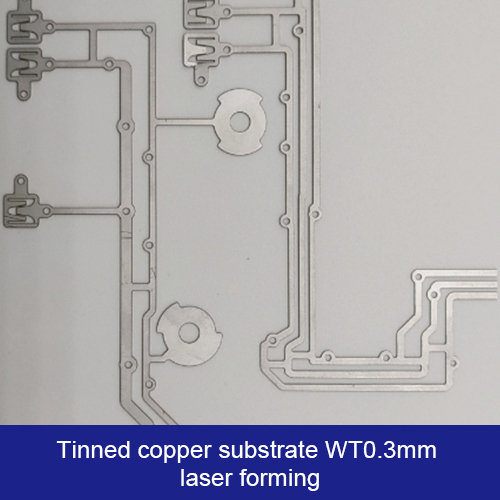
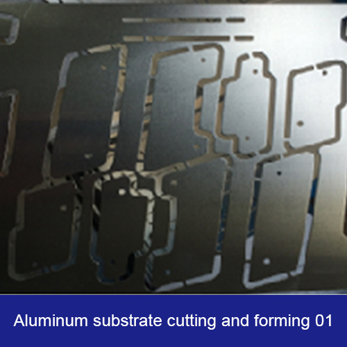
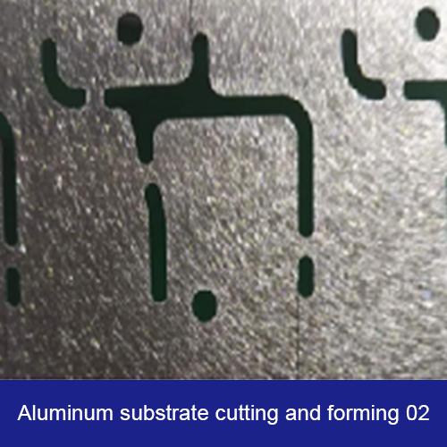
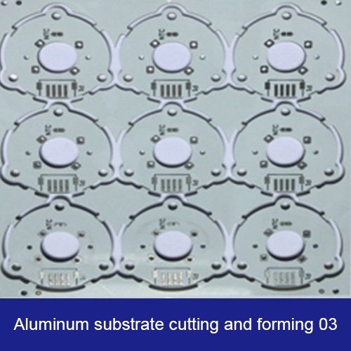
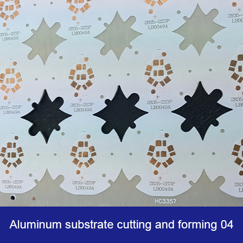
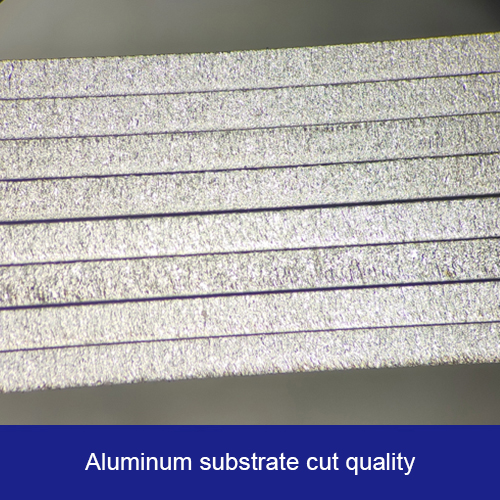
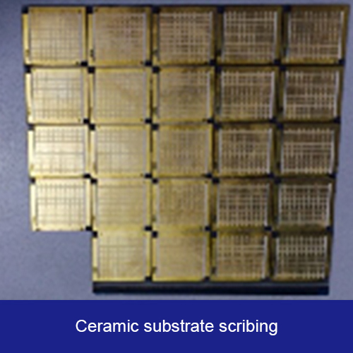
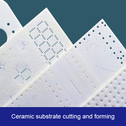
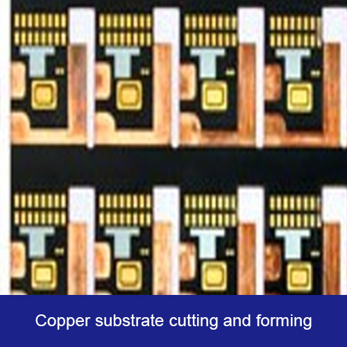
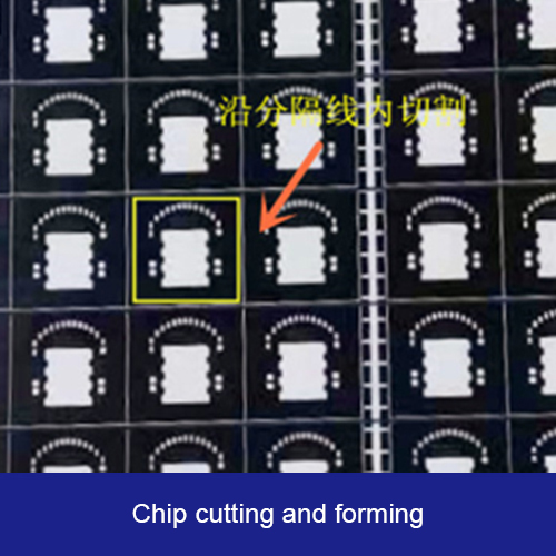
Sample display
Processing Materials:
- PCB aluminum substrate PCB aluminum substrate is a composite material consisting of a thin layer of dielectric insulation bonded to an aluminum base, offering excellent heat dissipation, mechanical stability, and dimensional accuracy for electronic circuit applications.
- PCB copper substrate PCB copper substrate is a high-conductivity material that provides superior electrical performance, excellent thermal transfer, and strong adhesion for electronic circuits, making it ideal for high-frequency and high-power applications.
- Ceramic substrate Ceramic substrate is a durable material with excellent thermal conductivity, high electrical insulation, and stability, making it ideal for high-power, high-frequency, and miniaturized electronic applications.
- Other related materials
Laser Specifications:
- Fiber-optic laser with wavelength 1030~1070±10nm
- Power Options: CW1000W, CW2000W, QCW150W, QCW450W, QCW750W
- Cutting Seam Width: 20~40μm
- Material Wall Thickness: 0~2.0±0.02 mm
Scope of Use
Precision laser micromachining for:
- Cutting, drilling, slotting, and scribing PCB substrates
- Processing aluminum, copper, and ceramic substrates
- Applications in semiconductor integrated circuits and precision PCB manufacturing
Processing Capabilities
- High machining accuracy: ≤±10μm
- Smooth incision with minimal heat-affected zone and few burrs
- Minimum product size: 100μm
Industries Served
- Electronics manufacturing
- Semiconductor industry
- PCB production and prototyping
Performance and Efficiency
Table size (mm): 600х800
WT: 0~2.0±0.02 mm
Maximum Operating Speeds:
- X, Y1, Y2 Axes: 500mm/s
- Z Axis: 50mm/s
Positioning Accuracy:
- ±3μm (X, Y1, Y2)
- ±5μm (Z)
Repeatability:
- ±1μm (X, Y1, Y2)
- ±3μm (Z)
Advanced Features
- Double station and visual positioning options
- Automatic loading and unloading system
- Customized vacuum adsorption fixture
- Slag and dust collection module with dust removal pipeline system
- Long and short focal length laser cutting head with sharp and flat nose options
Certified Quality
- ISO9001
- IATF16949
Design Excellence
- Ergonomic and compact design
- Self-developed 2D, 2.5D, and CAM software system for flexible production
- Intuitive interface with customizable software and hardware configurations
- Integrated safety explosion-proof treatment system